Jewar News: The country’s first DDIC OSAT unit will be established with an investment of ₹3,700 crore by HCL and Foxconn in the Yida area in Jewar. The project, which is expected to be operational by 2028, is expected to generate 3,500 jobs and contribute ₹45,000 crore to GDP.
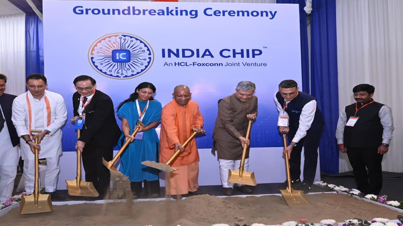
Jewar in the Yamuna Expressway Industrial Development Authority (YIDA) area is now emerging as the new center of the country’s semiconductor ambitions. The foundation stone of DDIC OSAT unit of India Chip Private Limited has been laid here. This is not just an industrial project, but is being considered a big step towards India’s technological self-reliance.
HCL–Foxconn Investment: Joint investment of over ₹3,700 crore
The project is being set up under a 60:40 joint venture between HCL Technologies and Foxconn. An investment of over ₹3,700 crore will create a state-of-the-art OSAT facility. This unit is expected to become operational by the year 2028. The plant will produce display driver chips used in smartphones, laptops, automobile systems and industrial electronics.
DDIC OSAT Unit: Processing capacity of 20,000 wafers per month
This will be the country’s first Display Driver Integrated Circuit (DDIC) OSAT unit. It will have a monthly processing capacity of 20,000 wafers. With this, the increasing demand for semiconductor components in India can be met domestically. Till now, India had to depend on imports for DDIC chips used in mobiles, TVs, laptops and automobile displays. This unit will reduce import dependence and strengthen domestic manufacturing.
Semiconductor Industry in UP: Yida area will become technology hub
The Yamuna Expressway area is already known for logistics and aerospace investments. Now with the addition of semiconductor industry, this area will develop as a high-tech manufacturing cluster. The project is expected to contribute approximately ₹45,000 crore to GDP per annum. This investment can establish Uttar Pradesh as a major semiconductor destination in the country.
Employment & Skill Development: More than 3,500 jobs
This mega project will generate more than 3,500 direct and indirect employment opportunities. Local youth will get an opportunity to work in advanced technical fields. Centers of excellence, research labs and simulation labs will be established under the project. Innovation will be promoted in the field of chip design and testing. Also, special training programs will be run in collaboration with local universities and technical institutes.
Make in India Boost: Big initiative towards self-reliant India
This project strengthens the vision of “Make in India” and “Self-reliant India”. Self-reliance in the semiconductor sector is extremely important from both economic and strategic points of view. This initiative in the YIDA (Yamuna Expressway Industrial Development Authority) area is a concrete step towards the goal of ‘Developed India 2047’. This foundation stone laying ceremony has emerged as a symbol of India’s technological confidence and industrial development.