Union Minister Ashwini Vaishnaw visited Dutch firm ASML, the world’s leading provider of lithography tools. He confirmed that India’s upcoming semiconductor fab in Dholera, Gujarat, will utilize ASML’s equipment for chip manufacturing.
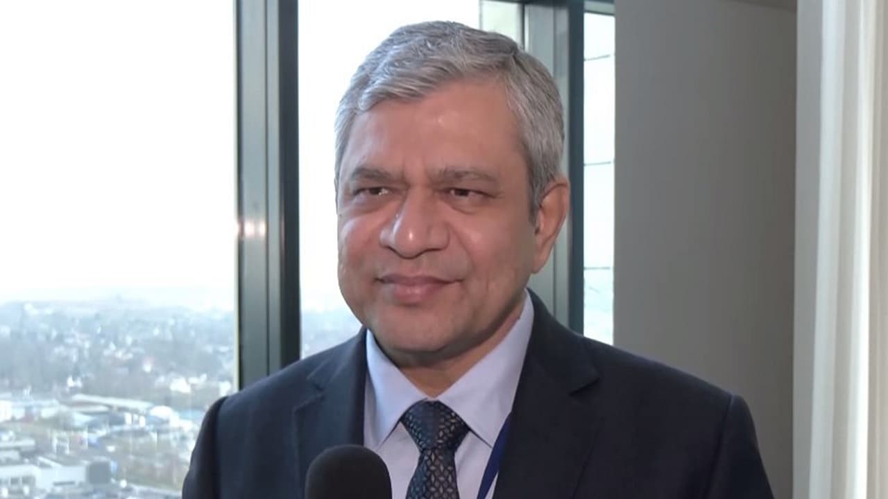
Union Electronics and Information Technology Minister Ashwini Vaishnaw on Friday explained the significance of his visit to Veldhoven in the Netherlands, stating that India has embarked on building a new semiconductor industry and that lithography remains the most complex and precision-intensive process in chip manufacturing.
Speaking to ANI, Vaishnaw said lithography, which involves printing circuits onto semiconductor wafers, is a critical step in the entire value chain. Noting that the semiconductor equipment maker ASML, based in the Netherlands, is the world’s leading provider of lithography tools and enables the manufacturing of almost every semiconductor chip globally, the Union Minister said that India’s upcoming semiconductor fabrication facility in Dholera, Gujarat will be using equipment from ASML.
“India has started a new semiconductor industry and in the entire semiconductor industry, lithography, which basically means printing the circuit on the wafer, is the most complex and the most precision work which is required to be done. ASML, here in Netherlands, is world’s leading provider of lithographic tool. They are the ones who enable practically every chip which is manufactured in the world. Our fab in Dholera will be using the ASML equipment,” Vaishnaw told ANI.
India’s Growing Role in Global Semiconductor Ecosystem
The Union IT minister said his visit to the Netherlands was aimed at understanding advanced technologies and strengthening collaboration, calling it a major opportunity for India. He noted that several global equipment manufacturers are now considering establishing a base in India, driven by the country’s strong design capabilities and skilled talent pool. Emphasising India’s growing role in the global semiconductor ecosystem, the minister said such engagements would help accelerate the country’s ambitions in high-tech manufacturing and innovation “So, I have come to visit here and understand their technology and this is going to be a major thing for India because many of the equipment manufacturers from all over the world are now looking at a base in India because of the design capabilities, because of the talent and because of the consistent policies of our Prime Minister,” Vaishnaw said.
The India Semiconductor Mission
India’s semiconductor journey reached a milestone in September 2025 as the first set of Made-in-India chips from a pilot line was presented to PM Modi by Union Minister of Electronics and Information Technology Ashwini Vaishnaw.
The India Semiconductor Mission was approved by the Union Cabinet in December 2021. With an outlay of Rs 76,000 crore, the programme aims to provide financial support for investments in semiconductor fabrication, display manufacturing and chip design to strengthen India’s integration into global electronics value chains.
Envisioned to be led by global experts in the Semiconductor and Display industry, ISM aims to build a strong semiconductor and display ecosystem, positioning India as a global hub for electronics manufacturing and design, while serving as the nodal agency for the efficient and seamless implementation of semiconductor and display schemes. (ANI)
(Except for the headline, this story has not been edited by Asianet Newsable English staff and is published from a syndicated feed.)