Union Minister Ashwini Vaishnaw unveiled a high-tech 2-nanometre chip by Qualcomm, celebrating India’s rapid progress in building an end-to-end semiconductor ecosystem and shifting from a back-office destination to a product development hub.
Union Minister for Electronics and IT Ashwini Vaishnaw on Saturday unveiled a high-tech 2-nanometre chip manufactured by Qualcomm. On the occasion, the minister underscored the country’s rapid progress in building an end-to-end semiconductor ecosystem.
A Hub for End-to-End Development
Speaking at the event, Vaishnaw said the development marks a shift from India’s earlier role as a back-office destination to a hub for end-to-end semiconductor product development, from customer product definition through silicon design, tape-out, and validation. “Our country is making major progress in the semiconductor manufacturing design and getting the entire ecosystem in our country. It’s a new industry,” he said.
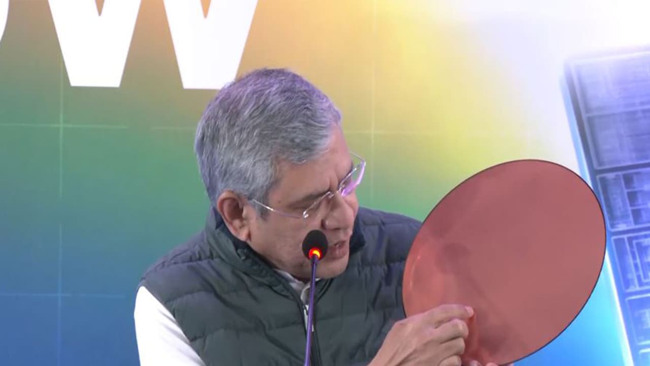
Inside the 2-Nanometre Chip
Holding a chip wafer in his hands, the minister described its capabilities and the precision manufacturing involved in it. The minister noted that the newly designed wafer contains approximately 20 to 30 billion transistors, with each die–a small square on the wafer–housing nearly 20 billion transistors. He explained that the chip integrates both a CPU and a GPU.
“The end product which comes out of this is this kind of module which comes out, which basically becomes an AI computer on the desktop of any person on the edge, which means within a camera, within a Wi-Fi router, or within a device on any machine or any moving car, automobile, train or aeroplane,” he said.
Fostering Semiconductor Talent
He lauded the Indian semiconductor talent developed under the Semicon mission. Vaishnaw credited India’s growing talent pipeline for reinforcing these technological advancements.
Under the Semicon India Mission 1.0, the government set a target to train 85,000 semiconductor professionals over a decade. By far, about 67,000 semiconductor engineers have been trained, he said.
According to the minister, semiconductor design education is now available at 315 universities and colleges nationwide, with students having access to advanced electronic design automation (EDA) tools. These students are designing chips, taping them out at the Semiconductor Laboratory in Mohali, and validating final products, a capability which, according to Vaishnaw, is rare globally. “Not many universities in the world, not many countries in the world, have this kind of model,” the minister said.
Future Roadmap: Semicon India Mission 2.0
Looking ahead, Vaishnaw said the government will soon roll out the Semicon India Mission 2.0, announced in the Union Budget by Finance Minister Nirmala Sitharaman. The next phase will prioritise semiconductor design, followed by equipment and materials manufacturing, deeper talent development for complete system-level design, and the expansion of fabrication and assembly, testing, marking, and packaging (ATMP) units.
He also said India’s roadmap to advance from current 28-nanometre manufacturing capabilities to 7-nanometre technology will be a key focus under Semicon 2.0, with preparations expected to be completed in the coming months. “We should be able to finally complete it within the next few months,” the minister said about Semicon 2.0, without giving a definitive timeline. (ANI)
(Except for the headline, this story has not been edited by Asianet Newsable English staff and is published from a syndicated feed.)