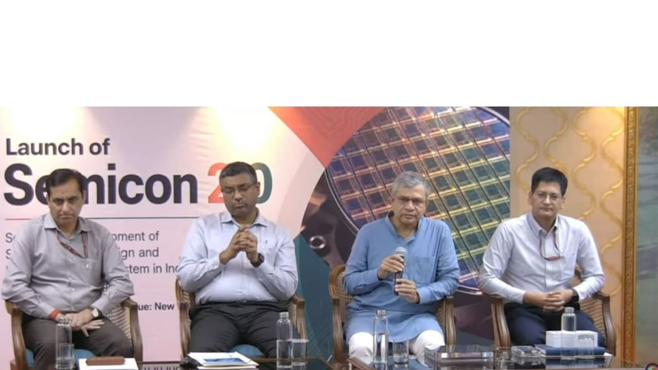
MeitY has detailed the eligibility for Semicon 2.0, requiring specific investment, revenue, and technology criteria for companies in chip design, fabs, and R&D. Indian ownership is mandatory for design firms. Support includes funding and incentives.
Companies seeking to participate in the government’s Semicon 2.0 programme will have to meet specific technology, investment, revenue and capacity requirements, depending on the segment of the semiconductor value chain, according to the scheme notified by the Ministry of Electronics and Information Technology (MeitY) on Monday.
Eligibility for Design Companies
For strategic semiconductor design, companies must be incorporated and headquartered in India, have a significant operational and manpower presence in the country and be owned and controlled by Indian citizens. They can apply either independently or in partnership with global companies, research organisations and academic institutions.
For commercial semiconductor design, companies must also be incorporated and headquartered in India and have a significant presence in the country. They must be owned and controlled by Indian citizens or Overseas Citizens of India (OCIs).
Financial Incentives for Design Firms
Eligible startups and MSMEs can get milestone-linked seed funding of 50 per cent of the project cost or Rs 15 crore, whichever is lower. Companies backed by venture capital or private equity can also receive equity co-investment.
The scheme also offers royalty financing to larger eligible companies. Under this arrangement, beneficiaries will pay 5 per cent of the net revenue generated from the product or technology until 1.5 times the government support is recovered.
For newly launched semiconductor intellectual property (IP), chips and system-on-chips (SoCs), eligible applicants can get a 9 per cent reimbursement on net sales for five years. The support will be capped at Rs 30 crore per application and Rs 120 crore per company, including group companies.
Requirements for Ancillary Facilities
For equipment R&D facilities, the minimum investment requirement is Rs 300 crore and minimum revenue requirement is Rs 120 crore. Raw-material facilities will need a minimum investment of Rs 50 crore and revenue of Rs 20 crore, while test and characterisation facilities will require Rs 100 crore investment and Rs 40 crore revenue.
Equipment and component manufacturing facilities will require a minimum investment of Rs 300 crore and revenue of Rs 120 crore.
These segments will be eligible for government support of 30 per cent of eligible capital expenditure.
Equipment and component manufacturers can also receive a production-linked incentive (PLI) ranging from 10 per cent to 2 per cent of the value of components sourced from domestic manufacturers for five years from FY2028-29. The overall support will be capped at 50 per cent of eligible capital expenditure.
Criteria for Semiconductor Fabs
Silicon Wafer Fabrication
The highest eligibility requirements have been set for silicon wafer fabrication plants. Projects must use 300-mm wafers, have a capacity of at least 40,000 wafer starts per month and use production-grade licensed technology. They must invest at least Rs 20,000 crore and have minimum revenue of Rs 7,500 crore in at least one of the previous three financial years.
The government will provide 40 per cent of eligible capital expenditure for such projects on a pari-passu basis.
Compound Semiconductor and Other Fabs
For compound semiconductor, photonics, sensor/MEMS and discrete semiconductor fabs, the minimum investment requirement is Rs 500 crore, revenue requirement is Rs 200 crore and capacity must be at least 500 wafer starts per month. These projects will receive 35 per cent support on eligible capital expenditure.
Packaging (ATMP/OSAT) and Advanced R&D
For ATMP/OSAT facilities, advanced packaging projects will require a minimum investment of Rs 1,000 crore and revenue of Rs 200 crore and will receive 35 per cent capex support. Legacy packaging projects with the same investment and revenue requirements will receive 25 per cent support.
The scheme also provides government support of up to 75 per cent of project cost for advanced semiconductor research and development, covering eligible capital and operating expenditure.
Mission Governance and Application
The notification follows the Union Cabinet’s approval of a Rs 1.27 lakh crore outlay for India Semiconductor Mission 2.0. The programme covers six pillars and 10 categories across the semiconductor value chain.
The India Semiconductor Mission will act as the nodal agency and assess applications based on technical and financial parameters, including process technology, project implementation capability, operational capability and off-take.
The scheme will initially remain open for applications for three years. (ANI)
(Except for the headline, this story has not been edited by Asianet Newsable English staff and is published from a syndicated feed.)