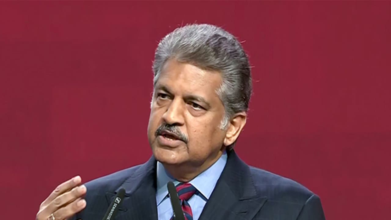
Anand Mahindra backs hands-on innovation as Mahindra University launches India’s second HackerFab, a student-led open-source semiconductor fabrication facility, to boost India’s domestic semiconductor capabilities with practical skills.
Mahindra Group Chairman and Mahindra University Chancellor Anand Mahindra has backed a hands-on approach to innovation, saying students should be encouraged to experiment, fail and build solutions themselves as India works to strengthen its semiconductor capabilities.
“Every great Indian innovation started with someone taking something apart to see how it worked. HackerFab gives students a license to do exactly that. To fail loudly, fix it, try again, no permission needed. That’s how you build a generation unafraid to build. That’s the India I want Mahindra University to help create,” Mahindra said. His remarks came as Mahindra University announced the launch of India’s second HackerFab, following the student-led HackerFab at IIT Bombay. The facility is the first university-sponsored, student-led open-source semiconductor fabrication facility in the country.
A Hands-On Approach to Fabrication
The initiative is aimed at giving students practical experience in semiconductor fabrication and helping develop technical skills needed to strengthen India’s domestic semiconductor capabilities. Led by students from the university’s B.Tech. in VLSI Design & Technology programme, the HackerFab will focus on developing low-cost fabrication equipment that can be used for education and research. The students will work on core semiconductor fabrication equipment, including a maskless photolithography system, RF sputtering chamber, spin coater and tube furnace.
The university said the hands-on model will allow students to work on semiconductor fabrication rather than limiting their learning to the design side of the technology. The initiative will also complement Mahindra University’s plans to establish a cleanroom facility for teaching and research.
Origins and Adoption of HackerFab
HackerFab was originally started in 2023 at Carnegie Mellon University’s Department of Electrical and Computer Engineering as an open-source initiative aimed at making semiconductor microfabrication more accessible through low-cost, student-built equipment. The model has since been adopted by institutions internationally and in India.
IIT Bombay students started India’s first student-built HackerFab in August 2025. They have developed prototypes of equipment used in semiconductor manufacturing, including systems for maskless lithography, spin coating, sputtering and furnace operations.
Building India’s Technological Self-Reliance
With the HackerFab, the university is seeking to bring semiconductor design, fabrication and research closer together. The initiative is aimed at giving students practical experience in building and testing fabrication equipment while developing the skills required for India’s growing semiconductor ecosystem.
The university said the focus is on developing engineers with both technical knowledge and practical experience as India works towards building domestic semiconductor capabilities and strengthening technological self-reliance. (ANI)
(Except for the headline, this story has not been edited by Asianetnews Editorial staff and is published from a syndicated feed.)