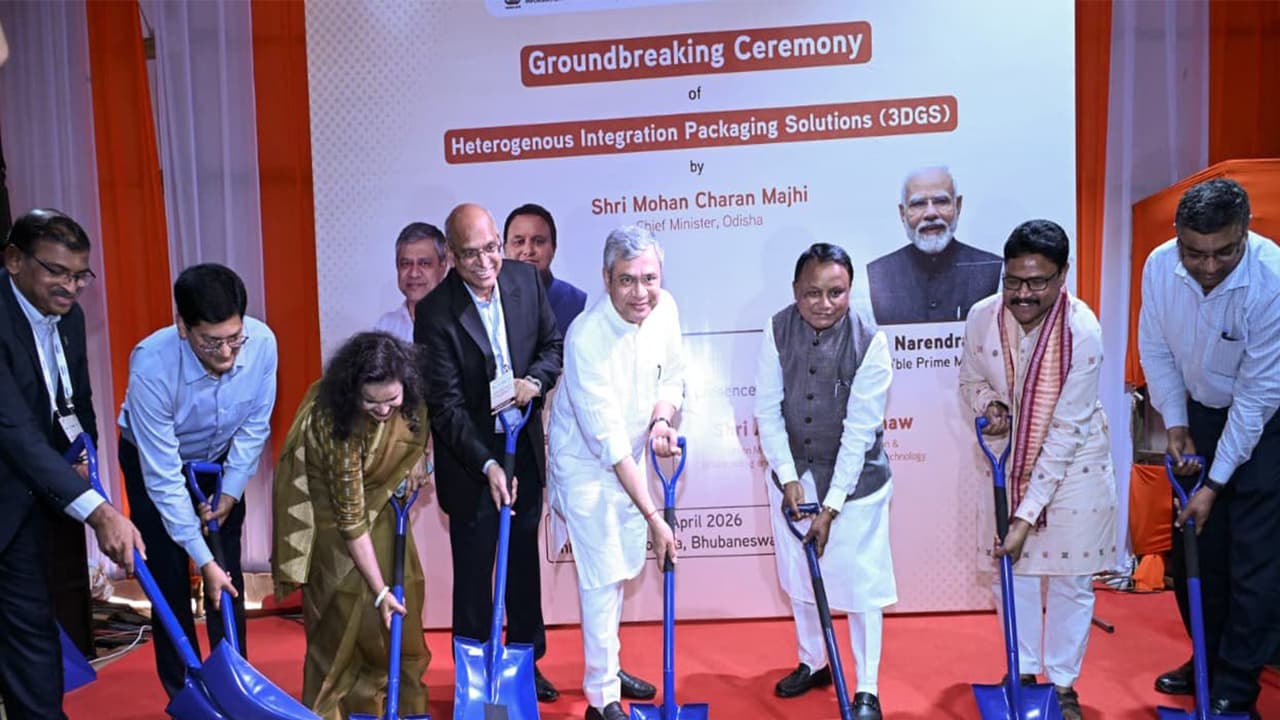
The foundation stone for India’s first advanced 3D chip packaging unit was laid in Bhubaneswar. The project, a significant step for ‘Atmanirbhar Bharat’, will use advanced 3D glass substrate technology and see an investment of Rs 2000 crore.
The foundation stone for the country’s first advanced 3D chip packaging unit was laid on Sunday at Info Valley, Bhubaneswar, Odisha. The project marks a significant step towards strengthening India’s domestic semiconductor ecosystem and advancing the vision of Atmanirbhar Bharat in high-end electronics manufacturing.
Advanced Technology and Future Plans
Union Minister for Electronics & IT Ashwini Vaishnaw said that the foundation stone of a semiconductor plant has been laid in Odisha on the occasion of Akshay Tritiya. He said the upcoming facility marks a significant step for high-tech manufacturing in the state, adding that he thanked Prime Minister Narendra Modi and Odisha Chief Minister Mohan Charan Majhi.
Calling it a matter of pride for Odisha, the Union Minister said the plant will be based on advanced technology, including the use of 3D glass substrate technology in chip manufacturing, which he described as a next-generation innovation in the semiconductor sector.
“On the occasion of Akshay Tritiya, the foundation stone of a semiconductor plant has been laid in Odisha. I want to thank PM Modi and CM Mohan Charan Majhi. A high-tech industry coming to Odisha is a matter of pride. This is an advanced technology. Normally, a silicone substrate is used in the manufacturing of chips, and now the technology of advanced 3D Glass substrate will be used, and the foundation stone of the first major plant using that technology has been laid in Odisha,” he said.
He added, “We will also work to double the capacity of the plant after the completion of the first phase of the plant. Several railway projects are underway in Odisha currently. Railway Stations in Puri, Bhubaneswar, Cuttack and other cities are being redeveloped.”
Investment and Employment Generation
Addressing the gathering, Chief Minister Mohan Charan Majhi described the project as a historic milestone for Odisha and the nation. He said that for the first time in India, an advanced 3D Glass Solutions semiconductor project is being established, bringing immense pride to the state. He noted that global technology leaders such as Intel, Lockheed Martin, and Applied Materials are associated with cutting-edge packaging technologies, and their interest in Odisha reflects the state’s growing industrial strength.
Majhi informed that the company is investing nearly ₹2,000 crore in the project and the facility is expected to produce 70,000 glass panels annually, along with 50 million assembled units and around 13,000 advanced 3DHI modules. He added that Odisha has emerged as the only state in the country where both India’s first compound semiconductor fabrication unit and first 3D glass substrate packaging facility are being established.
Meanwhile, speaking to reporters, the Odisha Chief Minister said, “This is happening for the first time in the country, and its construction will take place right here in Odisha. This is the future of semiconductor technology. This company is investing Rs 2000 crore in the first phase in Odisha. More than 2500 people will also get employment from this.” (ANI)
(Except for the headline, this story has not been edited by Asianet Newsable English staff and is published from a syndicated feed.)